The board
What is on the benchlink board, where it is, and how it connects to a Dabao.
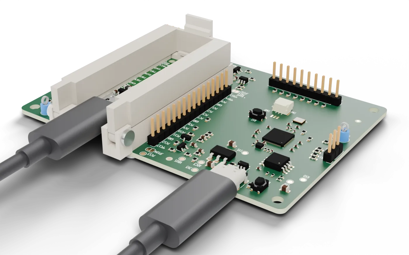
What it is
The bench link board holds a Dabao and connects it to your computer with one USB-C cable. An RP2350A bridges the Dabao’s console UART, drives its RUN, PC13 (PROG) and ON pins, and powers it through VSYS, with a current and voltage monitor on that feed. The benchlink command drives it.
benchlink is an independent tool. The Dabao and the Baochip-1x are Baochip’s.
The board is 95 x 66 mm, two layers, every part on the top side, with four M3 mounting holes on an 88.0 x 59.0 mm rectangle.
The safety rule
Nothing on the board can short or back-feed the Dabao, by design or by a firmware fault.
RUN,PC13andONare only ever pulled low, each through an N-MOSFET.- Nothing feeds the Dabao’s pin 40 (
VBUS) or pin 36 (3V3). - No part discharges a Dabao rail.
- No RP2350A pin reaches a Dabao pin except through a gate’s input, a MOSFET’s gate or at least 33 kΩ.
- An unpowered board does not load a powered Dabao, and the reverse.
Layout seen from above
Hold the board with its USB-C receptacle at the top.
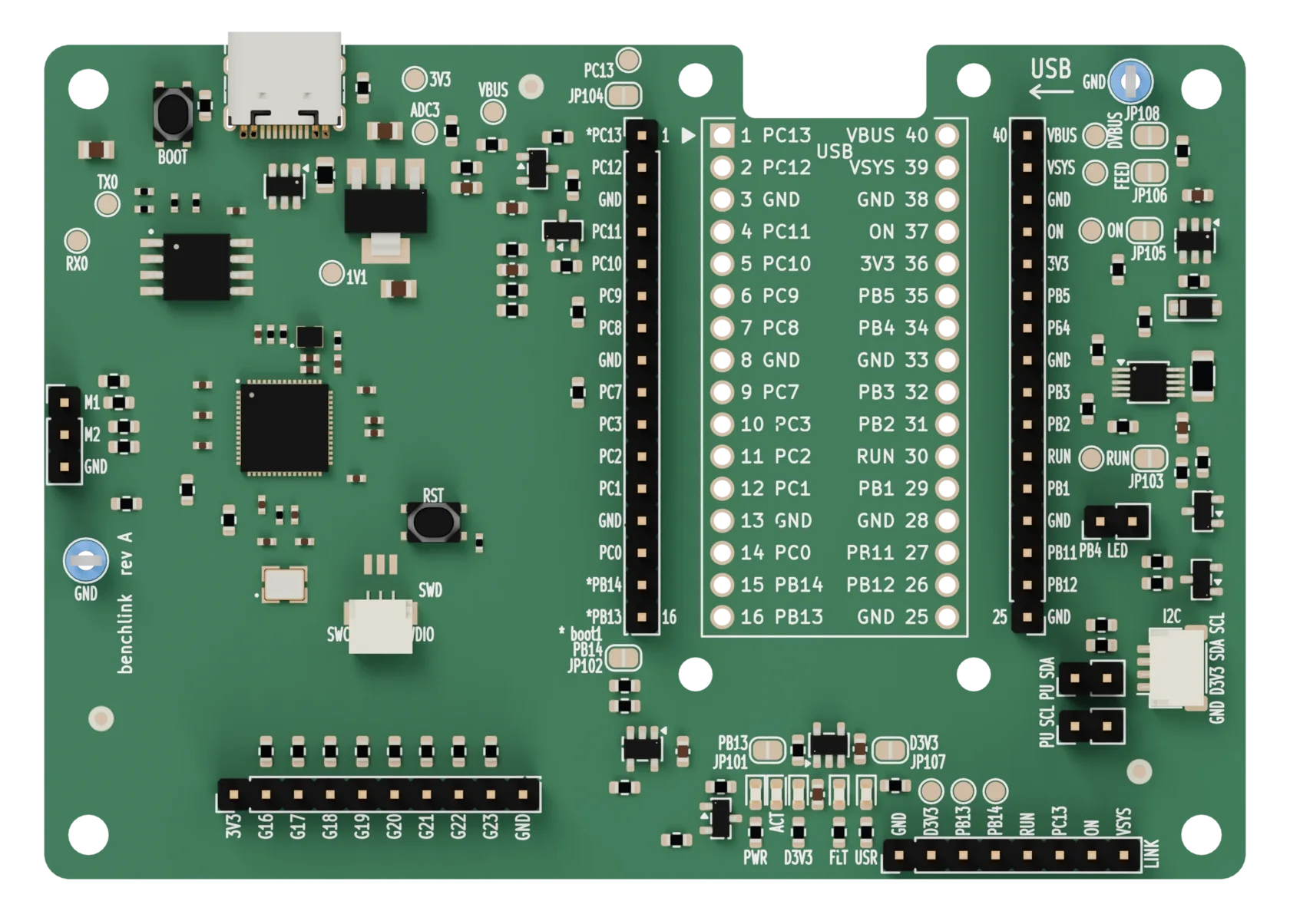
- Left: the USB-C receptacle and the
BOOTbutton at the top edge, the 3.3 V regulator and the flash below them, then the RP2350A with its 12 MHz crystal, theRSTbutton and the SWD connector. - Left edge: the debug UART test points (
TX0,RX0), the marker header, a ground loop. - Bottom left: the spare GPIO header.
- Right: the Dabao site, its USB-C end at the top, a breakout row each side.
- Top, above the site: a 14.5 mm notch, so a cable reaches the Dabao’s own USB-C.
- Right of the site: a ground loop in the top-right corner, then the power feed, the current monitor, the user-LED header and the I2C connector.
- Below the site: a strip kept free of parts for the cradle’s rear bar, then the status LEDs, then the link port on the bottom edge.
The Dabao site
The site has 32 holes under the Dabao’s pins 1 to 16 and 25 to 40, with names printed between the rows. The board is made in two builds, one for each kind of Dabao, both on these same 32 holes: Probes for a bare Dabao, Sockets for a Dabao with pin headers.
Build A, Probes
For a bare Dabao.
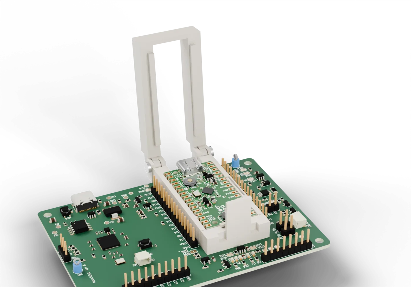
Each of the 32 holes holds a spring probe in a soldered sleeve, fitted when the board is made.
A printed cradle holds the Dabao down on the probes. Its frame is screwed to four holes around the site; a lid hinged at the USB-C end presses on the Dabao over its pin rows and latches at the back. The middle stays open, so the Dabao’s buttons can be pressed with the lid closed, and a USB-C plug reaches the Dabao’s own receptacle. A Dabao turned by 180° stops the lid from latching.
The cradle covers how they work, the case a case for the whole board, and Printing the parts yourself how to print them and the screws they take.
Build B, Sockets
For a Dabao with pin headers.
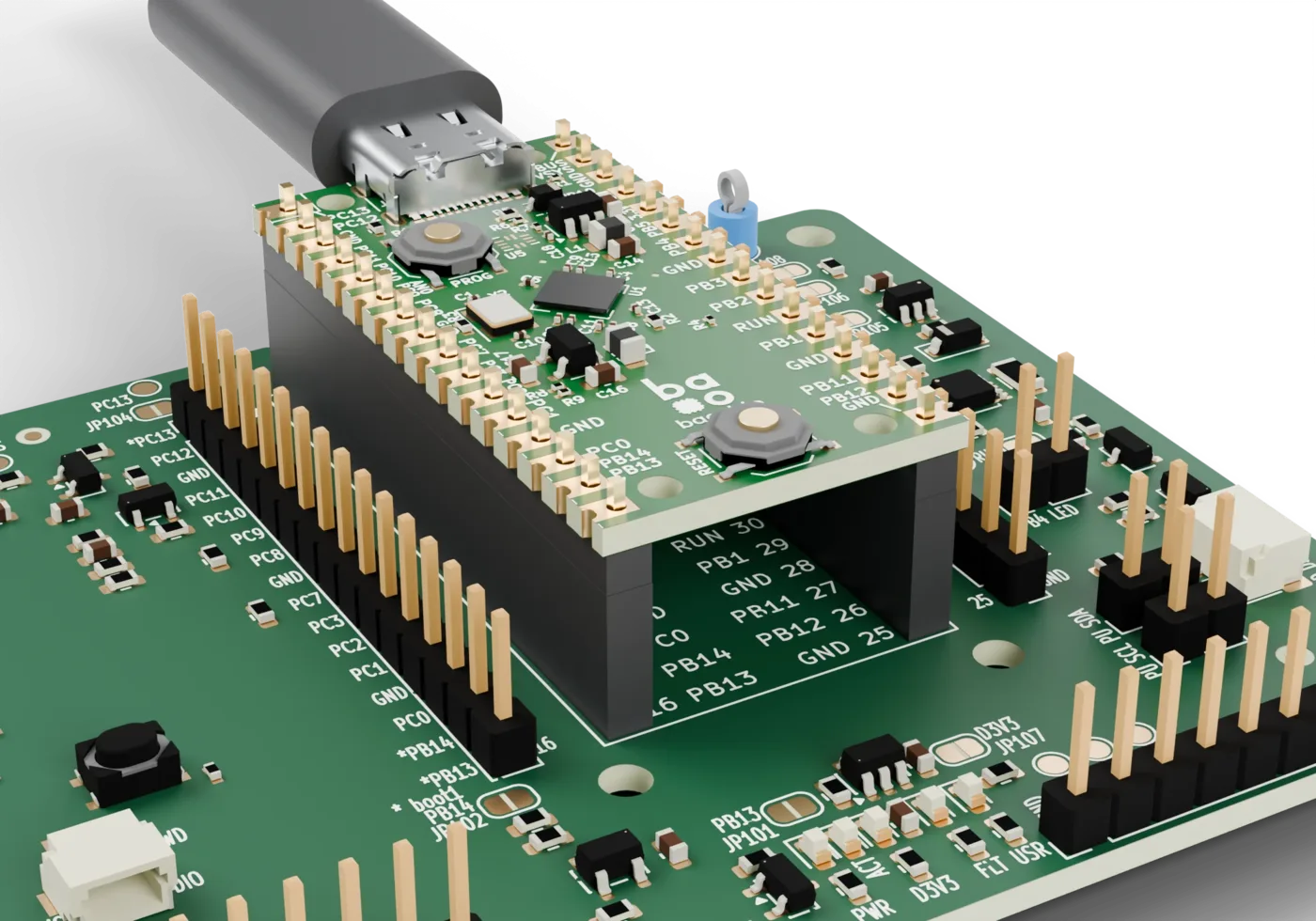
Two 1x16 low-insertion-force socket strips take a Dabao with headers. No cradle is needed. Plugging in takes about 12 to 16 N, pulling out 11 to 13 N. The Dabao’s underside is then about 11 mm above the board.
Warning
A Dabao with headers also fits turned by 180°. That puts its 5 V pin on a GPIO net. The Dabao’s USB-C end goes to the notch, where USB and an arrow are printed beside the site.
Breakouts
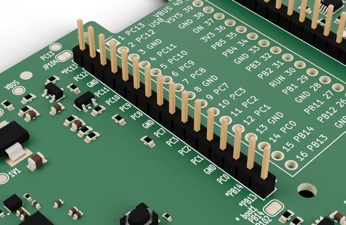
Two 1x16 rows carry every Dabao pin, each beside the Dabao pin it carries, named on both faces. The three pins that boot1 reserves are starred.
Power feed, limit and monitor
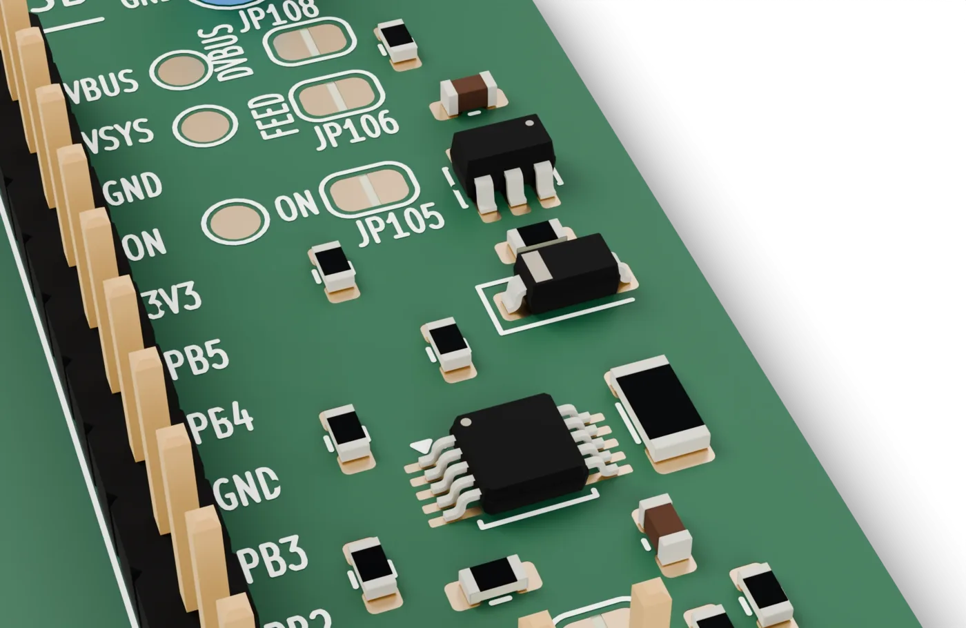
The board can power the Dabao from its own USB cable:
VBUS -> current-limited switch -> Schottky diode -> 0.1 Ω shunt -> Dabao VSYS- The switch limits the current to 314 mA at least, 353 mA typical, 397 mA at most. That leaves about 100 mA for the board itself within a USB 2.0 port’s 500 mA.
- An INA228 across the shunt measures the Dabao’s current and voltage, on I2C0 at address 0x40.
The board also reads the Dabao’s 3.3 V rail, the Dabao’s pin 40 and the board’s VBUS.
The supply and the lines to the Dabao are simulated in SPICE, with the makers’ models where they publish one: a cable plugged in hot, the feed starting a Dabao, a short on VSYS, the console line while the RP2350A is not driving it, and the three MOSFETs. The results are in the repository under hardware/sim. They are simulated, not measured.
The three control lines
| Line | Dabao pin | Held low means |
|---|---|---|
RUN |
30 | reset |
PC13 (PROG) |
1 | the PROG button pressed |
ON |
37 | both of the Dabao’s regulators off |
Released, each line floats, as with no board attached. The Dabao’s own buttons keep working.
The console runs at 1,000,000 baud: PB13 into the Dabao, PB14 out. The line into the Dabao idles high while the RP2350A is in reset or unpowered.
Status LEDs
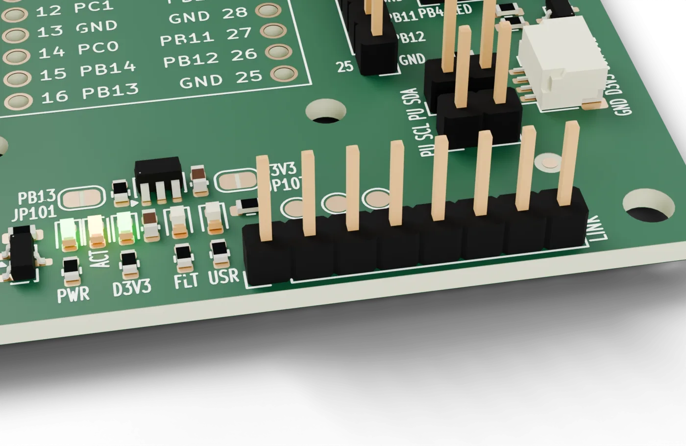
| LED | Lit when |
|---|---|
PWR |
the board has power |
ACT |
the firmware shows activity |
D3V3 |
the Dabao’s 3.3 V rail is up |
FLT |
the feed switch reports a fault |
USR |
the Dabao drives PB4, with the cap fitted on the user-LED header |
All five are lit from the board’s own 3.3 V.
Connectors
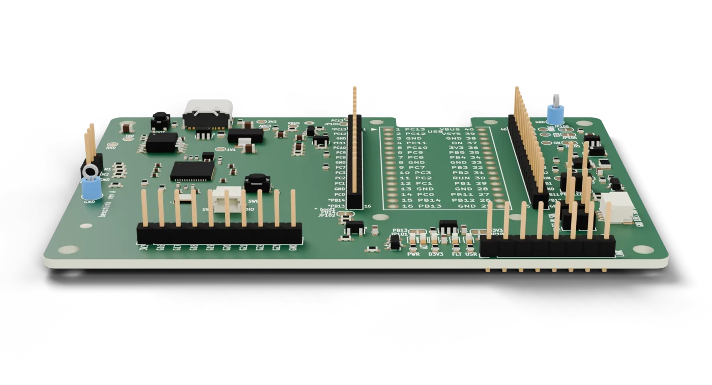
| Connector | Details |
|---|---|
| USB-C | USB 2.0, to the host; the only cable needed |
| I2C | four-pin JST SH on PB12 and PB11, supplied from the Dabao’s 3.3 V. A 4.7 kΩ pull-up per line, each switched by a capped header (PU SDA, PU SCL) |
| Markers | M1, M2, GND: 3.3 V inputs through 33 kΩ, to mark events in the current log |
| Spare GPIO | ten pins: 3V3, G16 to G23 (each behind 220 Ω), GND |
| Link port | 1x8 on the bottom edge: GND, 3V3, PB13, PB14, RUN, PC13, ON, VSYS |
| SWD | three pins, for the RP2350A |
| Ground loops | two, for probe clips |
Solder jumpers and test points
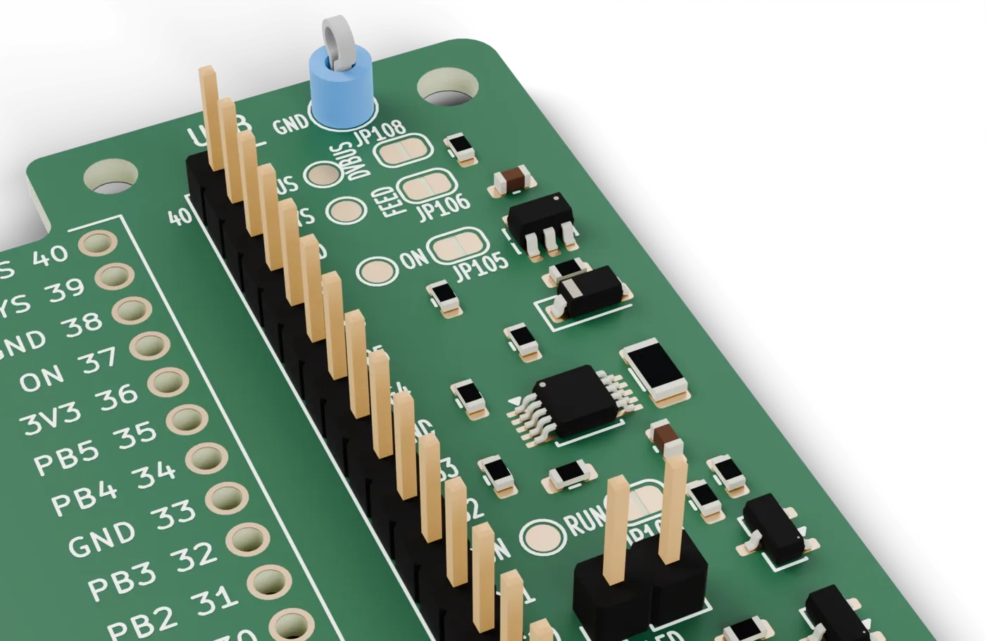
Every line to the Dabao passes a solder jumper, closed as made. Cut one to isolate that line. Each has a test point on the Dabao’s side.
| Line | Jumper | Test point |
|---|---|---|
PB13, console in |
PB13 JP101 |
PB13, above the link port |
PB14, console out |
PB14 JP102 |
PB14, above the link port |
RUN |
RUN JP103 |
beside the jumper |
PC13 |
PC13 JP104 |
beside the jumper |
ON |
ON JP105 |
beside the jumper |
VSYS, the feed |
FEED JP106 |
VSYS |
3V3, what the board hangs on it |
D3V3 JP107 |
D3V3, above the link port |
| pin 40, the sense divider | DVBUS JP108 |
beside the jumper |
The board’s own test points are 3V3, VBUS, 1V1, TX0, RX0 and ADC3.
VBUS and 3V3 name the board’s own rails; the Dabao’s are DVBUS and D3V3.
RP2350A pin map
For firmware work.
| Pin | Net | Use |
|---|---|---|
| GP0, GP1 | DBG_TX, DBG_RX |
debug UART (UART0), on test points |
| GP2, GP3 | MARK1, MARK2 |
marker inputs |
| GP4 | CONSOLE_TX |
UART1 TX, inverted, to the Dabao’s PB13 |
| GP5 | CONSOLE_RX |
UART1 RX, from the Dabao’s PB14 through a buffer |
| GP6 | RUN_GATE |
high holds the Dabao in reset |
| GP7 | PROG_GATE |
high holds PROG |
| GP8 | ON_GATE |
high switches the Dabao’s regulators off |
| GP9 | FEED_EN |
feed enable, active high |
| GP10 | FEED_FAULT_N |
feed fault, active low |
| GP11, GP15, GP24 | REV0, REV1, REV2 |
board revision; this board reads 011 |
| GP12, GP13 | MON_SDA, MON_SCL |
I2C0 to the INA228 |
| GP14 | MON_ALERT_N |
INA228 alert, active low |
| GP16 to GP23 | SPARE0 to SPARE7 |
spare GPIO header |
| GP25 | LED_ACT |
ACT LED |
| GP26 (ADC0) | SENSE_3V3 |
the Dabao’s 3.3 V rail, halved |
| GP27 (ADC1) | SENSE_DVBUS |
the Dabao’s pin 40, halved |
| GP28 (ADC2) | SENSE_VBUS |
the board’s VBUS, halved |
| GP29 (ADC3) | SPARE_ADC |
spare, on a test point |
The console into the Dabao is inverted in hardware, so the firmware sends inverted. A high gate pulls RUN, PC13 or ON low.